


Introduction
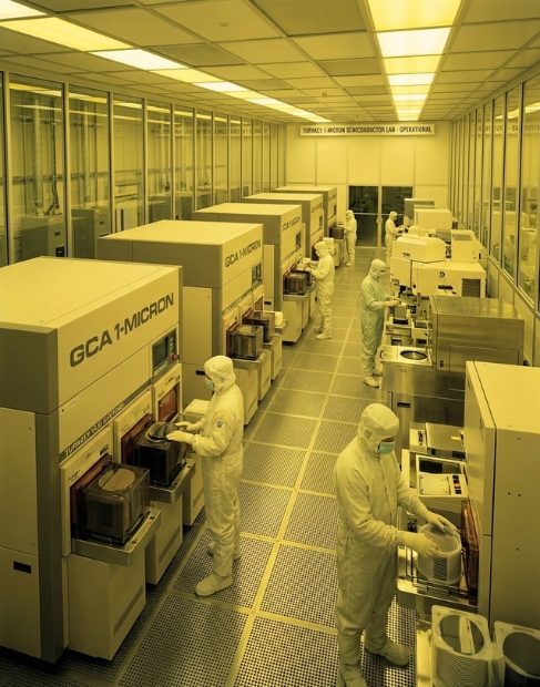
Ghadai Technology closes the "Lab-to-Fab" gap in Indian academia. We do not just supply equipment: we deliver a complete 1-micron teaching fab — cleanroom, utilities, tools, process, training and acceptance — under our single responsibility. Each lab is built so students can design, pattern, build, test and package real devices on campus, and the line can grow with further process modules as research needs expand. Our first line, for a private-sector education organisation, is under purchase order and in engineering and procurement.Our Turnkey Lab Models
1. For Tier-1 Universities (Research & IP Focus)
- Capability: A complete process flow — lithography, oxidation and diffusion, thin-film deposition, etching, metallisation, test and packaging.
- Outcome: A platform for publishable device research and deep-tech start-up incubation.
- Shared Facility: A resource for every engineering department on campus and for research collaborations with industry.
2. For Tier-2 & Tier-3 Universities (Skilling & Sustainability Focus)
- Capability: Acting as a "Feeder Node" for the industry. Students gain hands-on experience with vacuum systems, thermal processing and cleanroom safety.
- Operating Model: We help you set up the lab as a Section-8 entity, so the university can offer corporate training, research collaborations with local start-ups and testing services alongside teaching, within the lab's license and grant terms.
3. For Private Institutions (Commercial Training)
- Capability: High-throughput training centers designed for "Zero-to-One" skilling.
- Benefit: Train the cleanroom technicians and engineers India's semiconductor industry needs.
Technical Specifications
- Minimum Feature: 1.0 µm in vacuum-contact mode, on an i-line (365 nm) contact/proximity mask aligner, on 100 mm (4-inch) silicon wafers.
- Cleanroom: ISO 7 with ISO 5 laminar-flow zones, classified to ISO 14644-1 by accredited testing at handover; floor loading and vibration checked during site readiness.
- Safety Architecture: Gas life-safety design to the Gas Cylinders Rules, 2016 (and the SMPV(U) Rules for any bulk or cryogenic tank), with gas detection, segregated exhaust and scrubbing, safety showers, eyewash and hydrofluoric-acid exposure response; any PESO licence the site needs is in place before gases arrive.
- Acceptance: At handover, 1.0 µm lines resolved, overlay within ±1 µm and oxide thickness within ±5%. In the first year, our process lead works with your team to make working NMOS transistors, diffused resistors and MOS capacitors.